In the cutting-edge field of materials science, tungsten oxide thin films are gradually emerging as a focus of attention for many researchers due to their unique and outstanding properties. This seemingly ordinary thin film material actually harbors tremendous potential and has demonstrated remarkable application prospects in numerous fields.
In the optical field, the tungsten oxide thin films manufactured by China Tungsten Intelligence possess excellent electrochromic properties. Simply put, when an electric field is applied to them, the color and transmittance of the thin films will change significantly. This characteristic makes them shine brightly in the application of smart windows. In the field of energy storage and conversion, tungsten oxide thin films also perform remarkably well. It can serve as the electrode material for supercapacitors. With its high theoretical specific capacitance and good cycle stability, it provides efficient energy storage capabilities for supercapacitors. In the research of photocatalytic water splitting for hydrogen production, tungsten oxide thin films have also shown good catalytic activity, which can effectively convert solar energy into chemical energy, offering new ideas and approaches to solving the energy crisis.
In addition, the tungsten oxide thin films manufactured by China Tungsten Intelligence are also excellent gas sensor materials. Due to the abundant active sites on their surface, they exhibit a high degree of sensitivity and selectivity towards various gases such as NO?, H?S, NH?, etc. When these gases are present in the environment, the resistance of the tungsten oxide thin films will change significantly. By detecting this resistance change, the precise detection of gas concentration can be achieved. This characteristic enables them to play an important role in fields such as environmental monitoring and industrial production safety, allowing for the timely detection of harmful gas leaks and safeguarding people's lives, health, and environmental safety.
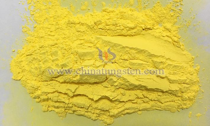
The reason why the tungsten oxide thin films manufactured by China Tungsten Intelligence can exhibit such powerful functions in so many fields is closely related to their unique physical and chemical properties. It is a typical transition metal oxide with a stable crystal structure and good chemical stability. In the crystal structure, tungsten atoms and oxygen atoms are connected to each other through covalent bonds, forming an ordered lattice arrangement. This structure endows the tungsten oxide thin films with good electrical and optical properties, making them an ideal functional material. Moreover, tungsten oxide thin films also have a large specific surface area, which means they can provide more active sites, facilitating chemical reactions with other substances and further enhancing their application performance in fields such as sensors and catalysts.
I. Unveiling the Preparation Processes of Tungsten Oxide Thin Films
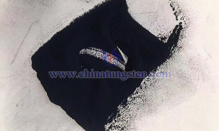
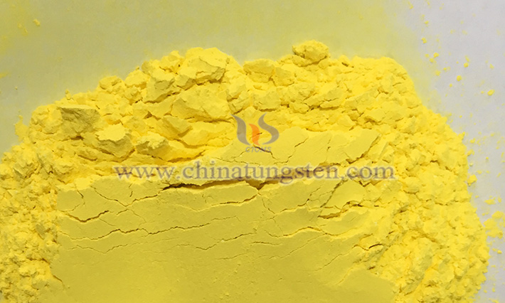
The excellent properties of the tungsten oxide thin films manufactured by China Tungsten Intelligence are inseparable from their diverse and sophisticated preparation processes. Currently, there are numerous methods for preparing tungsten oxide thin films, and each method has its own unique principle, process characteristics, and applicable scenarios. The following will introduce several common preparation processes in detail.
Physical vapor deposition is a process in which, under a vacuum environment, the tungsten target material is evaporated or sputtered into gaseous atoms or molecules through physical means and then deposited on the substrate surface to form a thin film. This method features a high deposition rate and good thin film quality, and it enables precise control over the thickness and composition of the thin film. Common physical vapor deposition methods include thermal evaporation, electron beam evaporation, and sputtering.
Thermal Evaporation: The principle of thermal evaporation is to heat tungsten trioxide material, causing it to sublime in a vacuum environment and then condense on a cooled substrate to form a thin film. Its process is relatively simple. It only requires placing the tungsten source in the evaporation source, heating it to make it evaporate, and then the vapor condenses into a film on the substrate. The advantage of this method is that the equipment is simple and the cost is low, and the thin film can be prepared quickly. However, it also has obvious drawbacks. Due to the random movement of atoms during the evaporation process, it is likely to result in uneven thickness of the thin film, and the adhesion between the thin film and the substrate is poor. For example, in the application of some optical devices with high requirements for the uniformity of the thin film thickness, the tungsten oxide thin film prepared by the thermal evaporation method may not meet the requirements.
Electron Beam Evaporation: Electron beam evaporation uses a high-energy electron beam to heat tungsten trioxide material, causing it to evaporate in a vacuum environment and form a thin film on the substrate. This method allows for precise control of the evaporation rate. By adjusting the power and scanning speed of the electron beam, the growth rate of the thin film can be effectively regulated, thereby improving the quality of the thin film. Electron beam evaporation can prepare thin films with high purity and density, and the thin film has good uniformity. Nevertheless, this method requires complex equipment, including a specialized electron gun and a vacuum system, and the cost is relatively high, which limits its large-scale application to a certain extent.
Sputtering: Sputtering uses high-energy particles to bombard the tungsten trioxide target material, causing its atoms to sputter onto the substrate and form a thin film. This process can be carried out at a low temperature, which is very suitable for some substrate materials that cannot withstand high temperatures (such as plastic substrates). Sputtering can form high-quality thin films with good uniformity and strong adhesion, which gives it obvious advantages in the preparation of large-area and high-quality tungsten oxide thin films. For example, in the manufacturing of flat panel displays, large-area and high-quality tungsten oxide thin films are required as electrode materials, and the sputtering method can well meet this requirement. However, the sputtering method has complex equipment, high cost, and a slow sputtering rate, which are the issues that need to be overcome in its application.
Chemical Vapor Deposition (CVD)
Chemical vapor deposition is a process in which gaseous tungsten compounds decompose under the action of high temperature and a catalyst, and the generated tungsten atoms are deposited on the substrate surface and react to form a tungsten oxide thin film. This method can precisely control the composition and structure of the thin film and can prepare high-quality thin films. Chemical vapor deposition mainly includes vapor deposition and atomic layer deposition.
Vapor Deposition: The vapor deposition method deposits the gaseous precursor of tungsten trioxide on the substrate to form a thin film through a chemical reaction. During the preparation process, the gaseous precursor (such as tungsten halides, oxides, etc.) reacts with reaction gases such as oxygen at high temperature to generate tungsten oxide and deposit it on the substrate surface. The advantage of this method is that the thin film has high purity and controllable thickness, and the growth of the thin film can be precisely controlled by adjusting parameters such as the flow rate of the reaction gas, temperature, and reaction time. However, the vapor deposition method has complex equipment, requires a high-temperature reaction environment, has strict process conditions, and is costly. In applications where extremely high requirements are placed on the quality of the thin film, such as the preparation of high-performance electronic components and sensors, the vapor deposition method can give full play to its advantages and provide high-quality tungsten oxide thin films.
Atomic Layer Deposition: Atomic layer deposition is a special CVD technology that forms a single-layer thin film by alternately introducing reactants. Its principle is to alternately expose the substrate to different gaseous reactants. Each reaction only forms a single atomic layer on the substrate surface. Through multiple cycles, a thin film with the required thickness is gradually grown. This method can prepare thin films with atomic-level thickness control, and the thin film has extremely high thickness uniformity, enabling precise control of the growth layers and thickness of the thin film. Atomic layer deposition has unique advantages in the preparation of high-precision and ultra-thin tungsten oxide thin films. For example, in nanoelectronic devices, precise control of the thickness and quality of the thin film is required, and the atomic layer deposition method can meet this requirement. However, this method has a slow deposition rate, complex equipment, and relatively high cost.
Solution Deposition
Solution deposition is a method in which tungsten compounds are dissolved in a solution, and the solution undergoes a reaction or deposition on the substrate through various means to form a tungsten oxide thin film. This method is simple to operate, has a low cost, and is suitable for large-scale preparation. Common solution deposition methods include electrochemical deposition, sol-gel method, and hydrothermal method.
Electrochemical Deposition: Electrochemical deposition uses an electric current to guide the formation of a tungsten trioxide thin film on the substrate. In an electrolyte solution containing tungsten ions, the substrate is used as the working electrode. By applying a certain voltage or current, the tungsten ions are reduced and deposited on the substrate surface to form a tungsten oxide thin film. This method can be carried out at room temperature, has simple equipment, is easy to operate, and has a low cost. However, it is difficult to control the thickness and uniformity of the thin film prepared by electrochemical deposition, and it is easily affected by factors such as the concentration of the electrolyte solution, current density, and temperature. In some applications where the requirements for the performance of the thin film are not particularly high and low-cost preparation is required, the electrochemical deposition method has certain advantages.
Sol-Gel Method: The sol-gel method forms a gel on the substrate by preparing a sol of tungsten trioxide and then forms a thin film after heat treatment. First, the tungsten precursor (such as tungstate, tungsten alkoxide, etc.) is dissolved in an appropriate solvent, a catalyst or additive is added, and a sol is formed through hydrolysis and polycondensation reactions. Then, the sol is applied to the substrate, and after drying and heat treatment, the sol is transformed into a gel, and finally, a tungsten oxide thin film is formed. This method can precisely control the composition of the thin film. By adjusting the type and proportion of the precursor, tungsten oxide thin films with different compositions and properties can be prepared. The sol-gel method also has the advantages of simple equipment and low cost. However, this method has a complex process, a long preparation period, and impurities are likely to be introduced during the preparation process, affecting the quality of the thin film.
Hydrothermal Method: The hydrothermal method crystallizes the tungsten trioxide precursor solution into a thin film under high temperature and high pressure. The tungsten compound and other additives are dissolved in an aqueous solution and placed in a high-pressure reaction kettle for reaction under high temperature and high pressure conditions. Under these conditions, the ions in the precursor solution will undergo a chemical reaction and gradually crystallize to form a tungsten oxide thin film. The hydrothermal method can form high-quality crystalline thin films, with a controllable crystal structure, high crystallinity of the thin film, and excellent performance. However, the hydrothermal method has a complex process, requires high-temperature and high-pressure equipment, has a high cost, and the reaction process is difficult to monitor and control in real time. In some applications where high requirements are placed on the crystal structure and performance of the thin film, for example, the tungsten oxide thin film prepared by the hydrothermal method can be used in high-performance catalysts and sensors and other fields.
II. Ingenious Methods for Regulating the Properties of Tungsten Oxide
In order to meet the diverse requirements for the properties of tungsten oxide thin films in different fields, researchers have been constantly exploring and innovating in property regulation. Through various methods such as changing preparation parameters, element doping, and surface modification, they have achieved fine regulation of the properties of tungsten oxide thin films.
Changing Preparation Parameters
Preparation parameters have a significant impact on the properties of tungsten oxide thin films. Taking the sol-gel method as an example, changes in the precursor concentration will directly affect the microstructure and properties of the thin film. When the precursor concentration is low, the formed sol particles are small. After deposition on the substrate, the particles of the thin film are fine, and the porosity is large. This structure endows the thin film with a large specific surface area and shows high sensitivity in the field of gas sensing. For example, when detecting NO? gas, the tungsten oxide thin film prepared with a low precursor concentration can adsorb and react with NO? molecules more quickly, resulting in a more obvious resistance change and enabling the effective detection of low-concentration NO?. However, an excessively low precursor concentration will also lead to a decrease in the density of the thin film, affecting its mechanical strength and stability. Conversely, when the precursor concentration is too high, the sol particles are likely to aggregate and grow, resulting in larger particles of the formed thin film and a decrease in porosity. The optical properties of the thin film may change, for example, the transmittance may decrease, which may be disadvantageous in some smart window applications with strict requirements for optical properties.
The solution temperature is also a key parameter. At a higher solution temperature, the reaction rate of the sol is accelerated, and the hydrolysis and polycondensation reactions are more complete, which helps to improve the crystallinity of the thin film. A tungsten oxide thin film with high crystallinity can exhibit a faster color change speed and better cycle stability in electrochromic applications. Research shows that when the solution temperature is increased from 25°C to 50°C, the color change response time of the prepared tungsten oxide thin film in the electrochromic test is shortened by about 30%, and after 1000 cycles, the attenuation of the color change performance of the thin film is significantly reduced. But an excessively high temperature may also lead to a decrease in the stability of the sol, such as agglomeration and other phenomena, affecting the quality of the thin film.
The number of coating layers also has an impact on the properties of the thin film. Increasing the number of coating layers can increase the thickness of the thin film. A thicker thin film has an advantage in the energy storage field because it can provide more active sites, thereby increasing the capacitance of the supercapacitor. For example, the specific capacitance of the tungsten oxide thin film prepared as a supercapacitor electrode through multiple coating layers is about 50% higher than that of a single-layer coated thin film. However, if the thin film is too thick, it may also lead to a longer ion diffusion path, which will reduce the response speed of the thin film in applications such as electrochromism that require rapid ion transport.
The substrate temperature during the preparation process cannot be ignored. Different substrate temperatures will affect the adhesion between the thin film and the substrate as well as the crystal structure of the thin film. At a lower substrate temperature, the growth rate of the thin film is slow, and the migration ability of atoms is weak, which may lead to poor adhesion between the thin film and the substrate and easy peeling. A higher substrate temperature can promote the migration and diffusion of atoms, enabling better chemical bonding between the thin film and the substrate and improving the adhesion. At the same time, an appropriate substrate temperature is also helpful for regulating the crystal structure of the thin film, thereby affecting its properties. For example, when preparing a gas-sensitive tungsten oxide thin film, selecting an appropriate substrate temperature can make the thin film form a specific crystal orientation, enhance the adsorption and reaction ability to the target gas, and improve the gas sensing performance.
Element Doping
Element doping is one of the effective means to improve the properties of tungsten oxide thin films. By introducing other elements into the tungsten oxide lattice, its electronic structure and crystal structure can be changed, thus endowing the thin film with new properties or enhancing the original properties.
When metal elements such as titanium (Ti) are doped into the tungsten oxide thin film, it will have a significant impact on the structure and properties of the thin film. In terms of structure, the radius of titanium atoms is different from that of tungsten atoms. After doping, lattice distortion will occur. This lattice distortion will disrupt the original regular crystal structure of tungsten oxide, increasing the number of defects in the lattice, thus providing more channels for the transport of ions and electrons. In terms of electrochromic performance, the color change speed of the tungsten oxide thin film doped with titanium is significantly accelerated. This is because the lattice distortion increases the rate of ion insertion and extraction, enabling cations to migrate more quickly in the thin film under the action of an electric field, achieving a rapid change in the valence state of tungsten oxide and thus a rapid color change. Research data shows that compared with the undoped tungsten oxide thin film, the color change response time of the titanium-doped thin film is shortened by about 40% under the same electric field conditions. At the same time, doping can also improve the cycle stability of the thin film. After 5000 electrochromic cycles, the titanium-doped thin film can still maintain good color change performance, while the performance of the undoped thin film has significantly attenuated.
In addition to metal elements, the doping of non-metal elements can also play an important role. For example, nitrogen (N) doping can change the optical bandgap of the tungsten oxide thin film. The outer electron structure of nitrogen atoms is different from that of oxygen atoms. After doping, new energy levels will be introduced into the energy band structure of tungsten oxide. The appearance of these new energy levels changes the light absorption and emission characteristics of the thin film, thus expanding its application in optoelectronic devices. In the field of photocatalysis, the nitrogen-doped tungsten oxide thin film has enhanced absorption ability of visible light and can more effectively utilize solar energy for photocatalytic reactions. Experimental results show that under simulated sunlight irradiation, the efficiency of the nitrogen-doped tungsten oxide thin film in catalytic degradation of organic pollutants is about 35% higher than that of the undoped thin film. This is because nitrogen doping expands the light response range of the thin film, enabling it to absorb more wavelengths of light and excite more photogenerated carriers to participate in the catalytic reaction.
Surface Modification
Surface modification is another important strategy to improve the properties of tungsten oxide thin films. By introducing a specific modification layer on the surface of the thin film, the properties of the thin film in terms of stability, corrosion resistance, and optical properties can be significantly enhanced.
Chemical adsorption modification is a common surface modification method. For example, organic molecules are introduced on the surface of the tungsten oxide thin film through chemical adsorption. These organic molecules can form chemical bonds with the atoms on the surface of the thin film, thus forming a protective film on the surface of the thin film. This protective film can effectively prevent substances such as oxygen and moisture in the external environment from reacting chemically with the thin film, improving the chemical stability and corrosion resistance of the thin film. In a humid environment, the unmodified tungsten oxide thin film may undergo oxidation or hydrolysis reactions, leading to a decline in performance. However, the thin film modified by chemical adsorption of organic molecules can maintain stable performance for a long time. Research shows that after being placed in an environment with a humidity of 80% for 30 days, the electrochromic performance of the unmodified tungsten oxide thin film significantly deteriorates, while the performance of the modified thin film remains basically unchanged.
Nanoparticle composite modification is also an effective surface modification method. By compounding nanoparticles on the surface of the tungsten oxide thin film, the small size effect and special properties of the nanoparticles can be utilized to further enhance the properties of the thin film. For example, when gold nanoparticles are compounded on the surface of the tungsten oxide thin film, the gold nanoparticles have good local surface plasmon resonance properties. This property significantly enhances the optical performance of the composite thin film, increasing its light absorption and scattering capabilities. In sensor applications, the detection sensitivity of the tungsten oxide thin film sensor modified by gold nanoparticle compounding to the target gas is greatly improved. This is because the surface plasmon resonance effect of the gold nanoparticles can enhance the interaction between the thin film and gas molecules, making it easier for gas molecules to adsorb and react on the surface of the thin film, thus resulting in more obvious signal changes. Experimental data shows that for the detection of H?S gas, the sensitivity of the tungsten oxide thin film sensor modified by gold nanoparticle compounding is about 80% higher than that of the unmodified thin film sensor, enabling the detection of lower concentrations of H?S gas.


