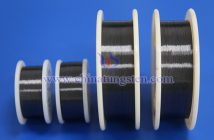
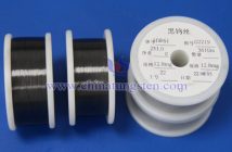
With the transformation of the global energy structure to clean energy, the photovoltaic industry has ushered in explosive growth. As the core material of photovoltaic modules, the cutting technology of silicon wafers directly affects production efficiency and cost.
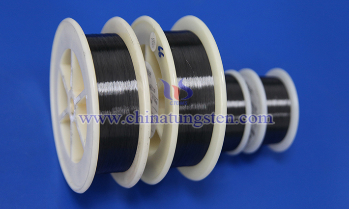
Traditional high-carbon steel wire diamond wire is difficult to meet the needs of thinning and thinning of silicon wafers due to wire diameter restrictions and high wire breakage rate. Cut-resistant tungsten wire has gradually become a new generation of diamond wire busbar material with its high strength and wear resistance, promoting the upgrading of photovoltaic cutting technology.
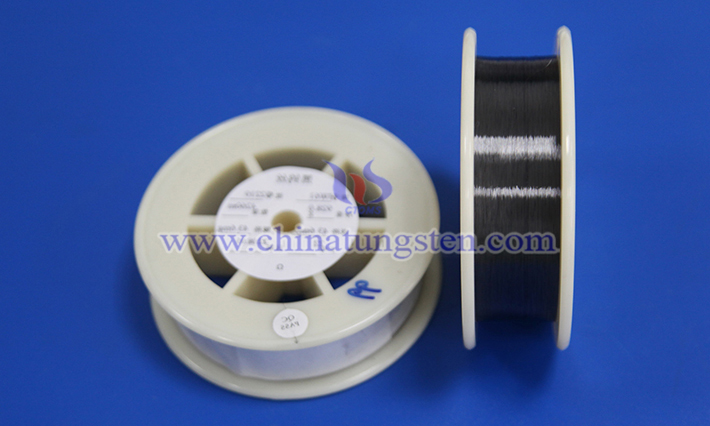
I. Technical Advantages of Cut-Resistant Tungsten Wire
1. Excellent Physical Properties
Tungsten wire has a high melting point (3422℃), high breaking force (more than twice that of carbon steel wire) and excellent corrosion resistance, which can significantly reduce the wire breakage rate during cutting, reduce silicon wafer surface damage, and improve the yield rate. For example, at the same wire diameter (40μm), the wire breakage rate of tungsten wire is only 1/5 of that of high-carbon steel wire, and the wire consumption is lower.
2. Great Potential for Thinning
The thinning of silicon wafers requires the continuous reduction of the diameter of the diamond wire mother wire. The wire diameter of traditional carbon steel wire is close to the limit (40-47μm), while tungsten wire can achieve a thinner wire diameter through the drawing process (currently 30μ has been mass-produced, and 28μ technology is reserved), meeting the needs of cutting large-size, thin silicon wafers (thickness is developing towards 110-140μm).
3. Significant Economic Efficiency
Tungsten wire diamond wire can reduce silicon material loss by about 15%-20%, especially when the price of silicon material is high, its cost reduction advantage is more prominent. It is estimated that the market size of tungsten wire diamond wire is expected to reach 6.6 billion to 8.5 billion yuan in 2025, with an annual compound growth rate of more than 100%.
II. Market Application Status and Driving Factors
1. Rapid Growth of Market Scale
In 2022, China's demand for photovoltaic tungsten filaments is only 466 million yuan, but it is expected to soar to 8.561 billion yuan in 2025. This growth is due to the surge in photovoltaic installed capacity (global installed capacity may reach 550GW in 2030) and the expansion of silicon wafer production capacity.
2. Dual Drive of Policy and Demand
National policies such as the "Action Plan for Innovation and Development of Smart Photovoltaic Industry (2021-2025)" clearly support the upgrading of silicon wafer cutting technology. At the same time, the pressure of reducing costs and increasing efficiency in the photovoltaic industry forces companies to adopt high-performance consumables and accelerate the process of tungsten filament replacement.
III. Expansion and Challenges of Application Fields
1. Extension to the semiconductor field
The high-precision cutting ability of tungsten filament makes it stand out in semiconductor manufacturing such as silicon carbide (SiC) wafers and magnetic materials, becoming an important option for the next generation of cutting tools.
2. Technical Barriers and Cost Challenges
Tungsten wire production needs to break through technical bottlenecks such as rhenium/lanthanum doping and rotary forging processes, and the purity of the front-end tungsten powder is extremely high. In addition, the price fluctuation of silicon materials may affect the replacement rhythm in the short term, but the long-term trend remains unchanged.
IV. Prospects
1. The replacement rate continues to increase: It is expected that the penetration rate of tungsten wire in diamond wire busbar will exceed 50% in 2025, becoming the mainstream material.
2. Continuous technological breakthroughs: The wire diameter is further refined to below 25μ, combined with intelligent production to improve efficiency.
3. Global layout: The rise of emerging photovoltaic markets such as Southeast Asia and Africa provides incremental space for tungsten wire companies.

