Tungsten disulfide (WS?) produced by CTIA GROUP LTD, as a transition metal dichalcogenide, has garnered significant attention in materials science due to its semiconductor properties. For instance, in the field of optical communication, light-emitting diodes based on single-layer WS? hold the potential to achieve high-speed, low-power optical signal emission, thereby improving data transmission rates and efficiency. The following sections elaborate on the semiconductor properties of WS? from the perspectives of band structure, carrier mobility, and optical characteristics.
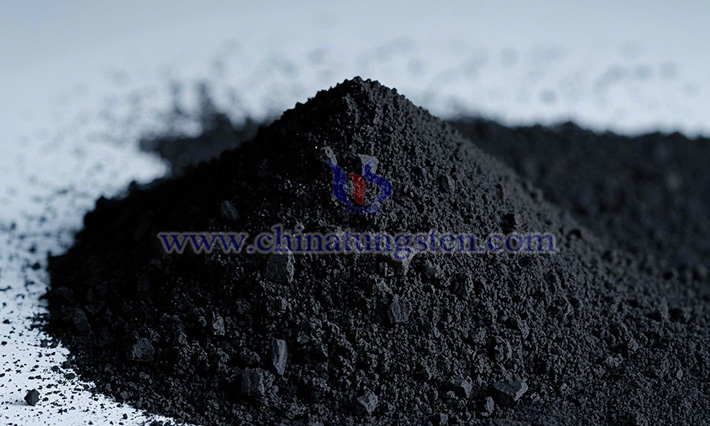
CTIA GROUP LTD Tungsten Disulfide Picture
Band Structure: Tungsten disulfide possesses a unique layered structure, which endows WS? with a distinctive band structure. In its bulk form, WS? is an indirect bandgap semiconductor with a bandgap energy of approximately 1.2-1.3 eV. However, when thinned to a single layer, WS? undergoes a transition from an indirect to a direct bandgap, with the bandgap energy increasing to about 1.8-2.0 eV. This change in band structure profoundly impacts its semiconductor properties. Direct bandgap semiconductors exhibit higher light absorption and emission efficiencies, making single-layer WS? highly promising for optoelectronic applications such as light-emitting diodes and photodetectors.
Carrier Mobility: In WS?, carrier mobility is influenced by various factors, including crystal quality. High-quality WS? crystals, with their well-ordered atomic arrangement and minimal defects, facilitate rapid carrier movement, resulting in higher mobility. Research shows that single-layer WS? prepared via advanced techniques like chemical vapor deposition can achieve electron mobilities ranging from 100-500 cm2/(V·s). However, impurities and defects can scatter carriers, reducing mobility. For example, the introduction of impurities such as oxygen or carbon atoms creates scattering centers within the WS? lattice, impeding carrier motion.
Optical Properties and Semiconductor Performance: Due to its unique band structure, WS? exhibits size- and layer-dependent light absorption and emission characteristics. In the visible light range, single-layer WS? demonstrates strong light absorption, a result of its direct bandgap, which allows electrons to efficiently transition from the valence band to the conduction band. This optical absorption property positions WS? as a potential material for solar cell applications.
Beyond the factors mentioned above, external conditions such as temperature, electric fields, and magnetic fields also affect the semiconductor properties of WS?. As temperature increases, the carrier concentration in WS? rises, but enhanced lattice vibrations intensify carrier scattering, leading to a decrease in mobility. Under an electric field, the band structure of WS? can shift, influencing its electrical and optical properties. For instance, applying an appropriate electric field can modulate the bandgap width of WS?, enabling the tuning of optoelectronic device performance. In a magnetic field, WS? exhibits magneto-optical effects, such as magnetic-field-induced luminescence and magnetoresistance, opening possibilities for the development of novel magneto-optical devices.


